Is Aeluma’s Technology Replicable? Rethinking the Moat in 2026
A recurring question from thoughtful investors: is the platform truly differentiated, or merely “good but replicable”?

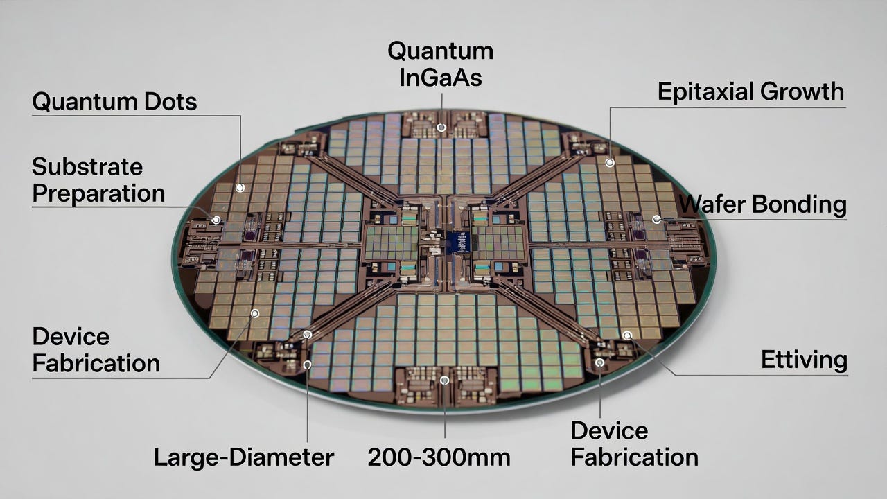
300 mm silicon wafer with III-V epitaxial layers, InGaAs, and quantum dots during heterogeneous integration processing—the scalable manufacturing foundation that defines Aeluma’s real moat.
It’s exactly the right question — just usually framed in the wrong way.
This Is Not a Device-Metric Story
Most debates zoom in on isolated specs — dark current, quantum efficiency, bandwidth, responsivity — and attempt to declare victory or defeat based on lab numbers.
That misses the real unlock.
Aeluma’s core value proposition is a manufacturing architecture: scalable III–V epitaxial integration (InGaAs, quantum dots, AlGaAs, etc.) directly on large-diameter 200–300mm silicon substrates, with a credible path to commercial economics and high-volume yields.
It is the combination of performance plus manufacturability that changes the outcome set.
Plenty of III–V devices look outstanding on small substrates, in university cleanrooms, or in carefully tuned demonstrations. The enduring constraint has always been scaling those materials economically while maintaining yield, reliability, and cost competitiveness at volume.
That is fundamentally a manufacturing and integration problem — not merely a physics problem.
What “Replicable” Actually Means in Semiconductors
In semiconductors, very little is theoretically “impossible” if one assumes unlimited time, capital, and talent.
The relevant questions are:
How long would true replication take?
At what capital intensity and burn rate?
Under what qualification and reliability constraints?
And by then, how deeply embedded is the incumbent in customer programs?
Aeluma’s platform has been refined over more than a decade, including sustained government-funded programs with DARPA, the U.S. Navy, NASA, and the DoE that require rigorous milestones, reproducibility, and formal data packages.
That history implies process maturity materially beyond the conceptual or “promising demo” stage.
Heterogeneous epitaxy at commercial scale requires mastery of:
Lattice mismatch and defect density control
Thermal expansion management across dissimilar materials
Multi-lot yield repeatability on 200–300mm wafers
Full reliability qualification (Telcordia/GR-468-style, plus defense/aerospace standards)
For even well-capitalized foundries, these are multi-year engineering campaigns — not single program cycles.
And there is an additional constraint many underestimate:
Capital can accelerate hiring. It cannot compress a decade-long process learning curve.
Deep materials integration is driven as much by tacit engineering learning curves as by formal IP language.
Recent Q2 FY2026 updates (released Feb 11) are instructive: management highlighted strong performance, quality, and yield of wafers fabricated with foundry partners and tested in-house, further supported by automated wafer probers from the recent test-asset acquisition. Wafers are yielding and performing as processes qualify into target markets.
That is execution progress — not lab hype.
The Hidden Friction: Defense, Security, and Supply Chains
There is another underappreciated layer of defensibility.
Once a technology embeds into defense-adjacent, security-sensitive, or strategic programs, barriers extend far beyond patents.
Approved vendor lists, facility clearances, ITAR-compliant flows, procurement pathways, and extended qualification regimes introduce real-time friction. Even technically capable fast followers can face multi-year delays simply navigating process approvals and compliance hurdles.
Patents matter — Aeluma’s IP portfolio totals approximately 35 issued and pending filings, including recent claims focused on scalable compound semiconductor manufacturing.
But accumulated tacit know-how from a decade of iteration around defect mitigation, growth parameters, and yield optimization is equally difficult to replicate.
You can fund headcount.
You cannot instantly recreate a process maturity curve.
Competitive Landscape: Separation, Not One-to-One Substitution
The giants — TSMC, GlobalFoundries, Intel — operate formidable photonics programs (e.g., Fotonix at GF, co-packaged optics initiatives at TSMC and Intel). Their center of gravity is silicon-native platforms optimized for datacenter transceivers and co-packaged optics.
Aeluma’s exposure differs:
SWIR sensing (defense, automotive, mobile)
Focal plane arrays
Quantum photonics (including quantum-dot-based lasers on 300mm through AIM Photonics)
Hybrid integrations where silicon-only approaches encounter intrinsic limitations
Recent awards — including NASA quantum-dot photonic contracts and RFSUNY/AIM Photonics funding — reinforce the company's position in performance-critical niches.
Replication risk is real. Large players have explored III–V on silicon for years.
However, Aeluma’s niche focus, government-validated head start, and current yield and qualification momentum create meaningful separation. In markets defined by long program and qualification cycles, timelines heavily favor the first mover, already converging on a manufacturable, qualifiable product.
The 2026 Investment Crux
The moat will not be proven by white papers, marketing decks, or isolated demos.
It will be proven through sustained execution across observable vectors:
Multi-lot yield stability at foundry scale
Reliability and qualification data packages delivered into defense and commercial programs
Successful foundry transfers and process qualifications
Customer design-ins transitioning into initial production ramps
Commercial embedment: early sales orders underway, RFQs evolving into pricing and planning, and scaled go-to-market expansion (bolstered by SVP Bouchaib Nessar)
Q2 FY2026 pointed directly at this trajectory:
NASA quantum-dot PIC contracts
RFSUNY/AIM Photonics funding for quantum-dot lasers on 300mm
Expanded manufacturing partnerships
Accelerated in-house test and validation capability
Strengthened commercialization leadership
Revenue came in at $1.3 million (primarily R&D milestones, with typical quarter-to-quarter variability in government contract timing). Cash and equivalents stood at $38.6 million with no debt — providing runway to execute qualification cycles without near-term balance sheet pressure.
If these milestones continue compounding — contract awards, design-ins, qualification data, foundry yield validation — the “replicable in the near term” bear case weakens structurally.
Skepticism is warranted if execution stalls.
But if manufacturability and qualification thresholds continue validating, valuation frameworks adjust accordingly.
Where Structural Value Is Created
Aeluma is past the phase of proving scientific viability.
The current phase is manufacturability, qualification, and embedment.
In semiconductor markets, that transition — if executed successfully — is where structural value is created.
(As always, this reflects my personal view, is not financial advice, and I remain significantly long $ALMU.)
wow a substack dedicated to a single stock props man
From your comment on Seekingalpha:
"At the material level, InGaAs is InGaAs. The physics advantage over silicon in SWIR does not change whether it is grown on InP or silicon. The question isn't whether it functions (it clearly does), but whether performance, defect density, dark current, and reliability meet target specs while achieving manufacturable yields on 200–300mm silicon."
So lets remove the substrate out of the equation. How does Aeluma create an equal or better InGaAs SWIR sensor than all the other big companies also making InGaAs SWIR sensors?